
Heat Transfer Fundamentals
Introduction to Heat Transfer
The objective of thermal management programs in electronic packaging is the efficient removal of heat from the semiconductor junction to the ambient environment. This process can be separated into three major phases:
1) Heat transfer within the semiconductor component package;
2) Heat transfer from the package to a heat dissipater (the initial heat sink)
3) Heat transfer from the heat dissipater to the ambient environment (the ultimate heat sink)
The first phase is generally beyond the control of the system level thermal engineer because the package type defines the internal heat transfer processes. In the second and third phases, the packaging engineer’s goal is to design an efficient thermal connection from the package surface to the initial heat spreader and on to the ambient environment. Achieving this goal requires a thorough understanding of heat transfer fundamentals as well as knowledge of available interface materials and how their key physical properties affect the heat transfer process.
Basic Theory of Heat Transfer
The rate at which heat is conducted through a material is proportional to the area normal to the heat flow and to the temperature gradient along the heat flow path. For a one dimensional, steady state heat flow the rate is expressed by Fourier’s equation:
Where:
k = thermal conductivity, W/m-K
Q = rate of heat flow, W
A = contact area
d = distance of heat flow
T = temperature difference
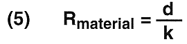
Thermal conductivity, k, is an intrinsic property of a homogeneous material which describes the material’s ability to conduct heat. This property is independent of material size, shape or orientation. For non-homogeneous materials, those having glass mesh or polymer film reinforcement, the term “relative thermal conductivity” is appropriate because the thermal conductivity of these materials depends on the relative thickness of the layers and their orientation with respect to heat flow. Another inherent thermal property of a material is its thermal resistance, R, as defined in Equation 2.
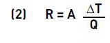
This property is a measure of how a material of a specific thickness resists the flow of heat. The relationship between kand R is shown by substituting Equation (2) into (1) and rearranging to form (3).

Equation 3 above shows that for homogeneous materials, thermal resistance is directly proportional to thickness. For non-homogeneous materials, the resistance generally increases with thickness but the relationship may not be linear.
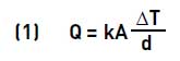
Thermal conductivity and thermal resistance describe heat transfer within a material once heat has entered the material. Because real surfaces are never truly flat or smooth, the contact plane between a surface and a material can also produce a resistance to the flow of heat. This contact plane is depicted in Figure 1. Actual contact occurs at the high points, leaving air-filled voids where the valleys align. The air voids resist the flow of heat and force more of the heat to flow through the contact points. This constriction resistance is referred to as surface contact resistance and can be a factor at all contacting surfaces.
The thermal impedance, θ, of a material is defined as the sum of its thermal resistance and any contact resistance between it and the contacting surfaces as defined in Equation (4).
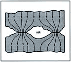
Figure 1a. Schematic representation of two surfaces in contact and heat flow across the interface.
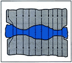
Figure 1b. Interface material compressed between two contacting surfaces.
This property is a measure of how a material of a specific thickness resists the flow of heat. The relationship between kand R is shown by substituting Equation (2) into (1) and rearranging to form (3)
Equation 3 shows that for homogeneous materials, thermal resistance is directly proportional to thickness. For non-homogeneous materials, the resistance generally increases with thickness but the relationship may not be linear.
Thermal conductivity and thermal resistance describe heat transfer within a material once heat has entered the material. Because real surfaces are never truly flat or smooth, the contact plane between a surface and a material can also produce a resistance to the flow of heat. This contact plane is depicted in Figure 1. Actual contact occurs at the high points, leaving air-filled voids where the valleys align. The air voids resist the flow of heat and force more of the heat to flow through the contact points. This constriction resistance is referred to as surface contact resistance and can be a factor at all contacting surfaces.
The thermal impedance, θ, of a material is defined as the sum of its thermal resistance and any contact resistance between it and the contacting surfaces as defined in Equation (4).
Surface flatness, surface roughness, clamping pressure, material thickness and compressive modulus have a major impact on contact resistance. Because these surface conditions can vary from application to application, the thermal impedance of a material will also be application dependent.
What Are Thermal Interface Materials?
Heat generated by a semiconductor must be removed to the ambient environment to maintain the junction temperature of the component within safe operating limits. Often this heat removal process involves conduction from a package surface to a heat spreader that can more efficiently transfer the heat to the ambient environment. The spreader has to be carefully joined to the package to minimize the thermal resistance of this newly formed thermal joint.
Attaching a heat spreader to a semiconductor package surface requires that two commercial grade surfaces be brought into intimate contact. These surfaces are usually characterized by a microscopic surface roughness superimposed on a macroscopic non-planarity that can give the surfaces a concave, convex or twisted shape. When two such surfaces are joined, contact occurs only at the high points. The low points form air-filled voids. Typical contact area can consist of more than 90 percent air voids, which represents a significant resistance to heat flow.
Thermally conductive materials are used to eliminate these interstitial air gaps from the interface by conforming to the rough and uneven mating surfaces. Because the material has a greater thermal conductivity than the air it replaces, the resistance across the joint decreases, and the component junction temperature will be reduced.
A variety of material types have been developed in response to the changing needs of the electronic packaging market. These materials can be categorized as follows:
Phase-Change Materials
THERMFLOW™ products provide a combination of grease-like thermal performance with pad-like convenience when used between high performance microprocessors and heat sinks.
- Can achieve less than 0.05°C- in 2/W thermal impedance
- Conform at operating temperature to minimize thermal path thickness
- Excellent surface “wetting” eliminates contact resistance
Phase-change materials behave like thermal greases after they reach their melt temperature. Their viscosity rapidly diminishes and they flow throughout the thermal joint to fill the gaps that were initially present. This process requires some compressive force, usually a few psi, to bring the two surfaces together and cause the material to flow. This process continues until the two surfaces come into contact at a minimum of three points, or the joint becomes so thin that the viscosity of the material prevents further flow. These materials do not provide electrical isolation because they may allow the two surfaces to make contact.
Thermal Gap Filler Pads
THERM-A-GAP™ gap fillers provide a family of low modulus (soft), thermally conductive silicone elastomers for applications where heat must be conducted over a large and variant gap between a semiconductor component and a heat dissipating surface.
- Soft silicone gel binder provides low modulus for conformability at low pressures
- Low modulus allows materials to make up for large tolerance stack ups
- Low pressure applications
Gap fillers are used to bridge large gaps between hot components and a cold surface. The gaps are not only large, but their tolerances can be +/–20 % or greater. This means that the gap filler must have sufficient pliancy to fill such spaces without stressing components beyond their safe limits. The thermal conductivity of these materials is in the moderate range and their use is typically limited to moderate-to-low power dissipation components.
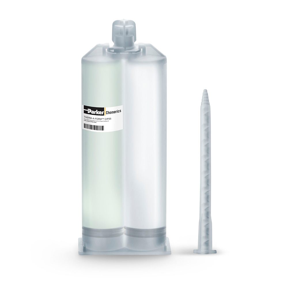
Cure In Place Thermal Compounds
THERM-A-FORM™ compounds are reactive, two-component silicone RTVs* that can be used to form thermal pathways in applications where the distance between a component and a cold surface is highly variable.
- Boron nitride or aluminum oxide-filled low modulus silicone resins
- Fill gaps ranging from 0.005 to 0.25 inch without stressing components
- Can cure at room temperature
- Localized encapsulating of components
*Room temperature vulcanizing materials.
Insulating Pads
CHO-THERM® insulating pads were developed as a user-friendly alternative to greased mica insulators to be used between discrete power devices and heat sinks.
- Silicone binder provides high temperature stability and good electrical insulation properties
- Glass mesh reinforcement provides cut-through resistance
- High mounting pressure required to minimize contact resistance
- U.L. Recognized
This class of product is characterized by high thermal conductivity, very high dielectric strength and volume resistivity. Pads must conduct very large heat loads from discrete power semiconductors to heat sinks, while providing long-term electrical insulation between the live component case and the grounded heat sink.
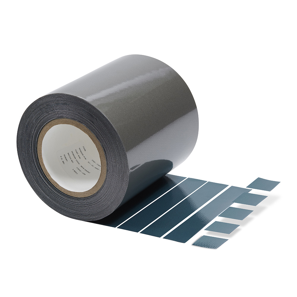
Thermal Tapes
THERMATTACH tapes are a family of acrylic and silicone pressure-sensitive adhesive tapes designed to securely bond heat sinks to power dissipating components.
- Acrylic based adhesives for metal or ceramic packages
- Silicone based adhesive for bonding plastic packages to heat sinks
- Ionically pure formulations for use inside component packages and on printed circuit boards
- Limited gap filling properties require reasonable surface flatness
- High shear strength at elevated temperatures
Thermal tapes are used primarily for their mechanical adhesive properties, and to a lesser extent for their thermal properties. The thermal conductivity of these tapes is moderate and their thermal performance in an application is dependent on the contact area that can be achieved between the bonding surfaces.
Thermal Properties
The key properties of interface materials are thermal impedance and thermal conductivity. What's the difference?
Thermal Impedance
This is the measure of the total resistance to the flow of heat from a hot surface through an interface material into a cold surface. Thermal impedance is measured according to the ASTM D5470 test method. Although the current version of this method is specific to high durometer insulating pad materials tested at high clamping forces, the method has been successfully adapted for use with low durometer materials as well as fluid compounds.
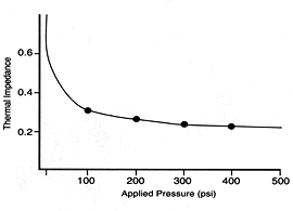
Thermal impedance can be measured using D5470 at several clamping forces to generate a pressure versus thermal impedance plot as shown in Figure 2. This type of data can be used to generate information about the ability of a material to conform to surfaces to minimize contact resistance. Care must be taken with this type of data because contact resistance is also highly influenced by surface characteristics. To minimize the impact of test equipment variations, this type of work is best performed with the same test surfaces for all materials being tested.
Figure 2. Thermal Impedance vs. pressure for CHO-THERM 1671 material.
Thermal Conductivity
Thermal impedance data measured according to ASTM D5470 can be used to calculate the thermal conductivity of an interface material. Rearranging Equation (4) to give Equation (5) and substituting into Equation (4) yields Equation (6).
Equation (6) shows that for a homogeneous material, a plot of thermal impedance (q) versus thickness (d) is a straight line whose slope is equal to the inverse of the thermal conductivity and the intercept at zero thickness is the contact resistance. Thickness can be varied by either stacking up different layers of the material or by preparing the material at different thicknesses.

Equation (6) shows that for a homogeneous material, a plot of thermal impedance (q) versus thickness (d) is a straight line whose slope is equal to the inverse of the thermal conductivity and the intercept at zero thickness is the contact resistance. Thickness can be varied by either stacking up different layers of the material or by preparing the material at different thicknesses.
Electrical Properties
The key properties of interface materials are thermal impedance and thermal conductivity.
Voltage Breakdown
This is a measure of how much voltage difference a material can withstand under a specific set of test conditions. This property is usually measured using ASTM D149 where a test specimen is subjected to ramped alternating current voltage such that dielectric failure is reached within twenty seconds after the start of the test.
Five specimens are tested and the average voltage breakdown is calculated and reported. The value is an average, not a minimum. Voltage Breakdown can be converted to Dielectric Strength by dividing the voltage breakdown value by the specimen thickness where the dielectric failure occurred. This test is an indication of the ability of a material to withstand high voltages, but does not guarantee how a material will behave over time in a real application. The value is influenced by several factors.
Humidity and elevated temperature will reduce the voltage breakdown because absorbed water will degrade the electrical properties of the material. The size of the test electrode will affect the observed breakdown voltage. A larger test electrode will typically yield a lower breakdown voltage. The presence of partial discharge, as well as mechanical stresses imposed on the interface material, also reduce voltage breakdown.
Volume Resistivity
Volume resistivity is a measure of the bulk electrical resistance of a unit cube of a material. When determined per ASTM D257, volume resistivity can give an indication of how well an interface material can limit leakage current between an active component and its grounded metal heat sink. As with voltage breakdown, volume resistivity can be significantly lowered by humidity and elevated temperature.
Elastomeric Properties
The key properties of interface materials are thermal impedance and thermal conductivity. Interface materials exhibit properties typical of highly filled elastomers, namely compression deflection, compression set and stress relaxation.
Compression Deflection
Unlike foams, a solid elastomer can not be compressed under normal compressive loads. As a compressive load is applied, the material is deformed but the volume of the material remains constant.
Stress Relaxation
When a compressive load is applied to an interface material, there is an initial deflection followed by a slow relaxation process whereby some of the load is relaxed. This process continues until the compressive load is balanced by the cohesive strength of the material.
Compression Set
Compression set is the result of stress relaxation. After a material has been subjected to a compressive load for an extended time, part of the deflection becomes permanent and will not be recoverable after the load is reduced.
CUSTOMER CASE STUDIES
Customers from a wide variety of industries look to Parker Chomerics to provide flexible, effective and reliable EMI shielding and thermal interface solutions.
SIGN UP FOR THE eNEWSLETTER
By signing up, you'll be the first to know:
- New product releases
- Updated support documentation and articles
- Existing product notifications
- The latest white papers, videos, and much more!

© Parker Hannifin Chomerics Division
World Headquarters
77 Dragon Ct., Woburn, MA 01801
781-935-4850