
Very High Frequency EMI Shielding Solutions for 5G Telecom Applications
October 17, 2022
Most will be familiar with the headline promises of 5G, such as the possibility of downloading a 2-hour film in 3 seconds (instead of 6 minutes with 4G). However, before these marketing soundbites become reality, there is much work to complete. 5G wireless technology is pledging to deliver higher multi-Gbps peak data speeds, ultra-low latency, more reliability, massive network capacity and increased availability. The resulting elevated performance and improved efficiency will empower new user experiences and connect new industries. With 5G, the full potential of the Internet of Things (IoT) can finally be realized through the connection of machines, objects, devices, and people.
At present, major players in the telecom arena are working hard to overcome a variety of technical barriers and deliver on 5G’s potential. Much of this focus is on unique EMI shielding techniques and materials to control Electromagnetic interference (EMI) and improve Electromagnetic Compatibility (EMC).
Different frequency bands
The next generation 5G wireless network seen in the advertisements is not the 5G available today. To understand why, it is necessary to set out the three different signal frequency bands.
Today’s 5G is essentially an advanced version of 4G. It has a little more capability, but it operates on the same frequencies (700 MHz to 2.6 GHz). Although there is a mid-range frequency band available of 2.5 to 6 GHz, the true promise of 5G and its potential to transform the world will take place in the ultra-high frequency arena (25 to 50 GHz), close to the bottom of the millimetre wave band.
One of the problems is a general lack of definition for the ultra-high frequency range. And this is just one issue of many. For instance, short transmission lengths of metres rather than kilometres are inherent with 5G. It could be that achieving the full potential of 5G will require more local network infrastructure, perhaps in the form of micro antennas placed on building rooftops or streetlamps (small cell sites), which are likely to be more compact than previous-generation solutions. There will be considerably more transmit/receive points.
One way to maintain a strong signal is to boost the power, but this has the negative consequence of generating heat in integrated circuits (ICs) and on printed circuit boards (PCBs). Reportedly, 5G signals even have problems negotiating obstacles such as trees in full leaf and tinted windows. Work to overcome these issues is therefore taking place concurrently with device and infrastructure development to help speed time-to-market.
Electromagnetic Interference, also known as EMI, is a disturbance produced by an external source, either man-made or naturally occurring, that can impact an electronic component or device via electromagnetic induction or capacitive coupling. No matter what the source may be, whether it be naturally occurring like lightning or man-made like heavy machinery, EMI is an undesirable byproduct of our surroundings and in an ideal environment, would not be present at all.
Electromagnetic interference shielding, commonly referred to as EMI shielding, is the use of incorporating certain materials into the design of an electronic device to prevent both external signals from entering and disrupting the device’s internal circuitry and internal signals from exiting and interfering with other surrounding electronics. The science behind engineering materials with EMI shielding properties is by no means simple and requires a thorough understanding of a variety of disciplines, including materials science and electromagnetic theory.
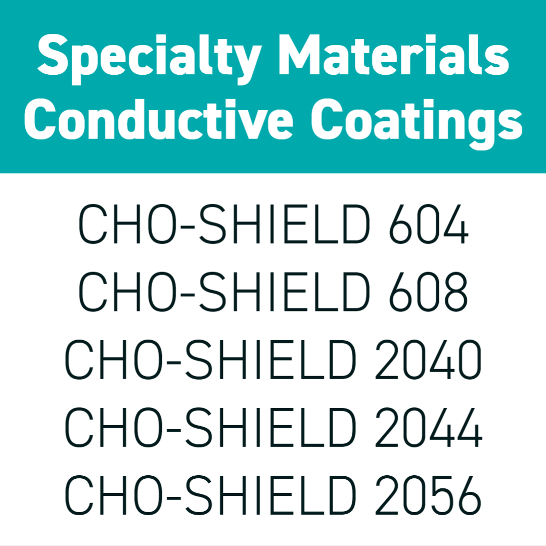
Parker Chomerics has developed CHO-SHIELD, a unique line of conductive coatings for specific use in real-world 5G EMI shielding solutions. Each distinct conductive coating is filled with a particular conductive material (i.e. nickel, gold, copper) and employs one of four resin types: acrylic, epoxy, polyester, or polyurethane. The coatings’ unique individual characteristics, albeit similar at their core, give each product in the line a specialized application. Moreover, all CHO-SHIELD coatings boast EMI shielding properties that help electronic devices/equipment meet global Electromagnetic Compatibility (EMC) requirements in the 5G market.
Specific conductive coatings focused for use in the 5G marketplace which were evaluated in this paper are as follows:
Test methods
In the past, the entire CHO-SHIELD family of products have been tested extensively for their EMI shielding properties, more specifically by utilizing industry standards ASTM-D4935 and IEEE-STD-299 over frequency bands spanning from 30 MHz to 40 GHz. While a solid understanding of the EMI shielding properties of CHO-SHIELD materials over these particular frequency bands has and always will be pertinent, our society is growing increasingly interconnected and, in turn, employing more and more of the electromagnetic spectrum for its electronic devices. As such, there is an increasing need for materials capable of EMI shielding at higher frequencies. That being said, high frequency EMI shielding testing has seldom been done in the past, so established test methods are anything but commonplace.
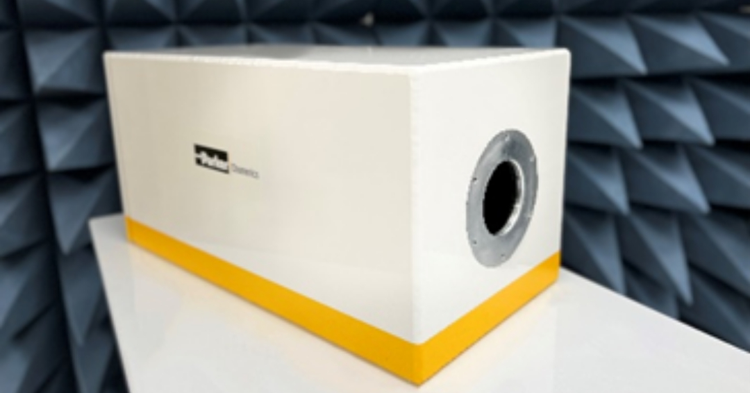
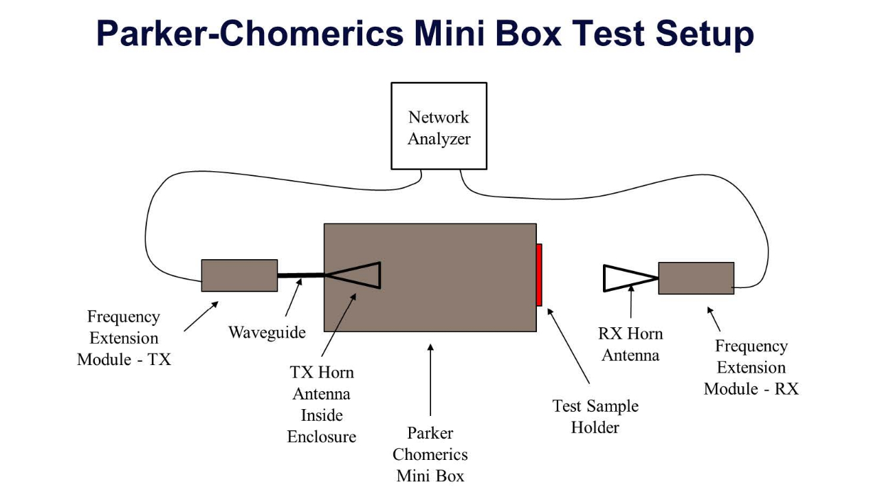
Being the first choice in EMI shielding solutions for the 5G marketplace, Chomerics material science and technical expertise has focused on EMI materials for higher frequency applications (> 18GHz). In order to accommodate the growing need for high frequency shielding effectiveness measurements, Parker Chomerics has developed a wholly unique and novel test method and setup for this exact purpose: the high frequency shielding effectiveness test enclosure, or the Parker-Chomerics “Mini Box” for short.
At first glance, the Mini Box does not appear to be elaborate. Its simplicity, however, is wherein its power lies. The test setup is in fact, a small scale IEEE-STD-299 test setup – it’s as simple as that.
Developing a new test method was necessary to evaluate shielding effectiveness at frequencies up to 115GHz. Typical large shielding effectiveness test chambers conventionally used for SE testing cannot be used due to equipment cable lengths and standard test equipment. Transfer Impedance test methods are not useful above 1-10GHz due to test fixture and test sample size.
Test samples
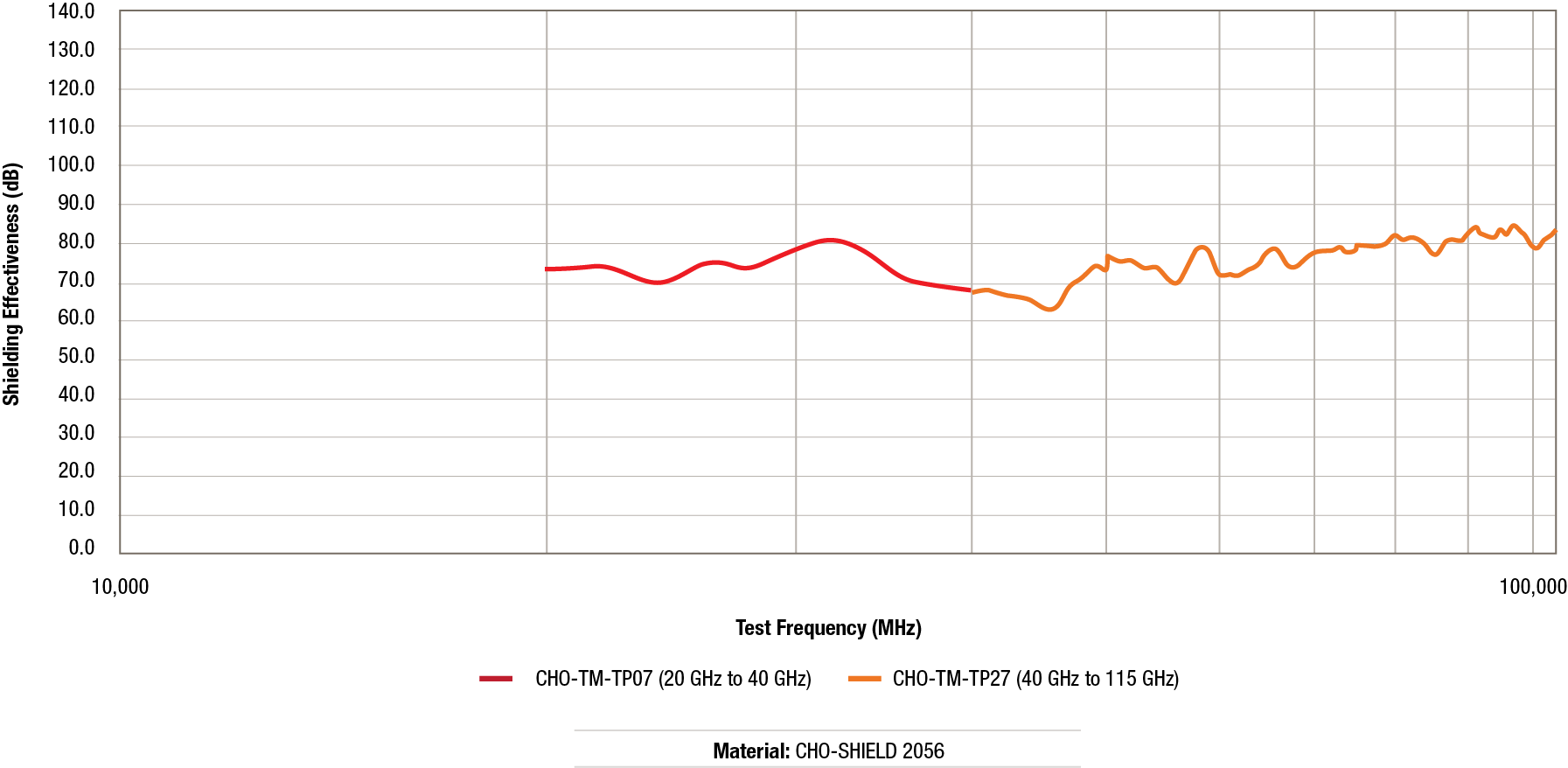
The CHO-SHIELD conductive coatings were applied to a plastic disk made from Ultem. The plastic disk is 5.25 inches in diameter. Using Ultem materials enables testing to be done using a plastic with appealing permittivity and permeability values that will not affect the test data. Application of the conducive coating was accomplished using typical recommended spray methods to achieve the recommended coating thickness. The benefit to this test sample size is that the very same test sample can be used for testing to ASTM D4935 AND IEEE-STD-299 using either the main test chamber or the Parker Chomerics Mini Box. This results in test data from 30MHz to 110GHz using the very same test sample. This paper focuses on the 18GHz to 115GHz frequency range. Test data below 18GHz is published in other media and not included.
IEEE STD 299 Test Using Test Chamber 18GHz to 40GHz
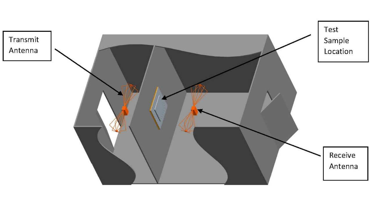
The IEEE STD 299 style testing is broken up in two test setups. First, Parker Chomerics main test chamber is used for testing frequencies from 18GHZ to 40GHz (Sometimes used down to 800MHz). Second, Parker Chomerics Mini Box is used for testing frequencies 40GHz to 110GHz (covered in the next section).
IEEE STD-299 was created to measure the shielding effectiveness of general room sized shielded encloses. This test standard was adapted to test materials. Parker Chomerics test chamber (shown below) is a fully welded steel chamber 12 x 20 feet in size with two sections and a common wall. The same test sample is positioned on the access panel on the common wall. One side of the test chamber holds the transmit test equipment and antenna and the other side holds the receive equipment and antenna.
The IEEE STD-299 tests performed in this test chamber utilizes a conventional spectrum analyzer, amplifiers, and antennas adequate to cover the desired frequency range.
IEEE STD 299 Test Using Mini Box 50GHz to 115GHz
The core principles of this innovative Mini Box test method are rooted in SE methodology and 2-port thru parameters. Utilizing a Keysight N5225A Network Analyzer, the transmission coefficient, specifically S12, is measured twice: once with the material in place on the Mini Box and once with nothing whatsoever in between the two antennas (IEEE-STD-299 Open Reference). Basic SE methodology tells us to find the difference between these two transmission coefficient readings in order to determine the shielding effectiveness of the material in question. As highlighted below, the Mini Box was more than successful in producing shielding effectiveness values for the entire family of CHO-SHIELD materials.
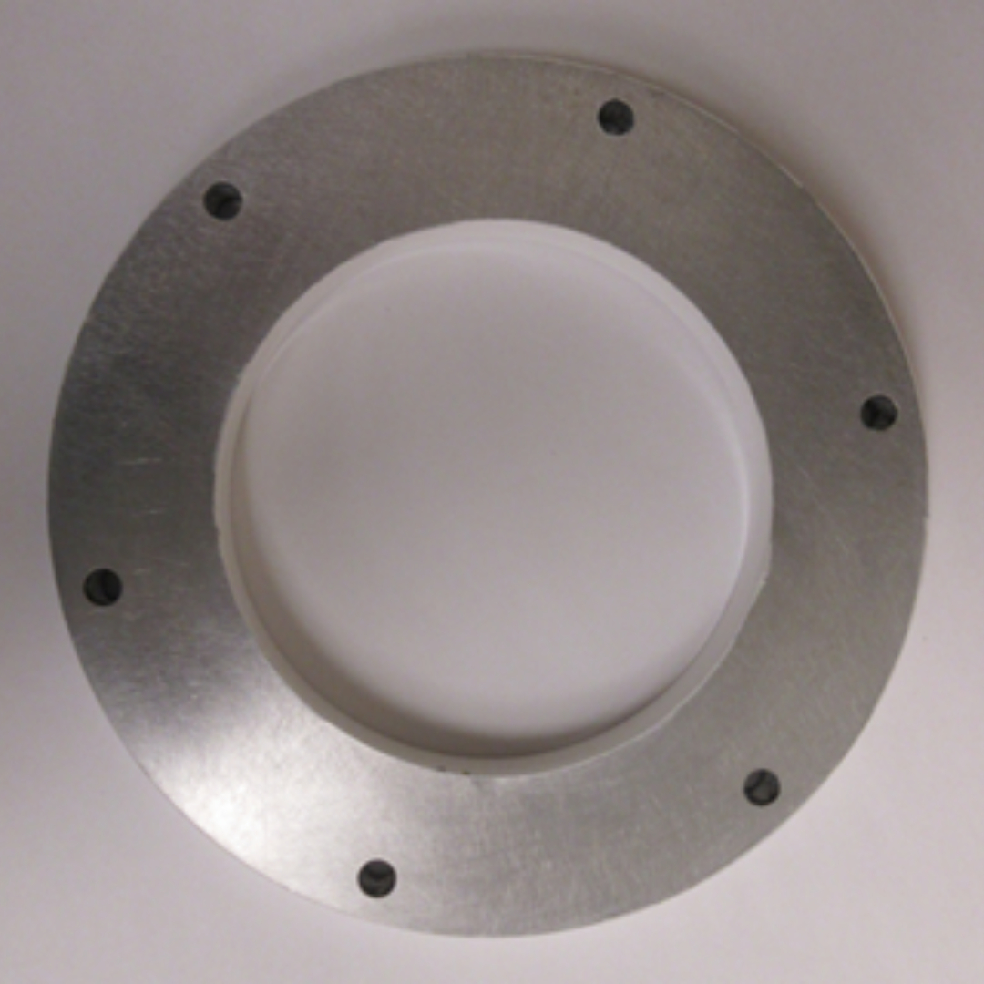
Here again, the very same test sample is positioned across the 3.5 inch aperture at the front of the enclosure. The 3.5-inch opening allows for any of the CHO-SHIELD materials to be mounted directly to the Mini Box itself with the assistance of plastic screws and a compression ring (shown below) with a 4-inch inner diameter is used to hold and compress the test sample in place.
One antenna, serving as the transmitting antenna, is affixed to the opposite end of the opening inside the enclosure. Another antenna, naturally functioning as the receiving antenna, is placed outside of the Mini Box in close proximity to the material under test. The Mini Box is constructed using ½ inch thick aluminum which is continuously seem welded and thin microwave absorber material lines the inner walls of the enclosure. The structure of the Mini Box and the placement of the antennas allow for shielding effectiveness values of EMI shielding materials to be easily obtained.
One of the most noteworthy features of the Mini Box test method and setup is its ability to measure the shielding effectiveness of the CHO-SHIELD materials over three distinct millimeter wavelength frequency bands, specifically the Q, V, and W bands. Ultimately, by incorporating three separate sets of antennas, frequency extension modules, waveguides, and feed-thru adapters, the mini box test method is capable of capturing the shielding effectiveness values associated with a material anywhere between 30GHz and 115GHz, all with an impressive 85dB of dynamic range.
The IEEE STD-299 test performed in this Mini Box utilizes a Network Analyze, frequency extension modules and antennas adequate to cover the desired frequency range as shown below.
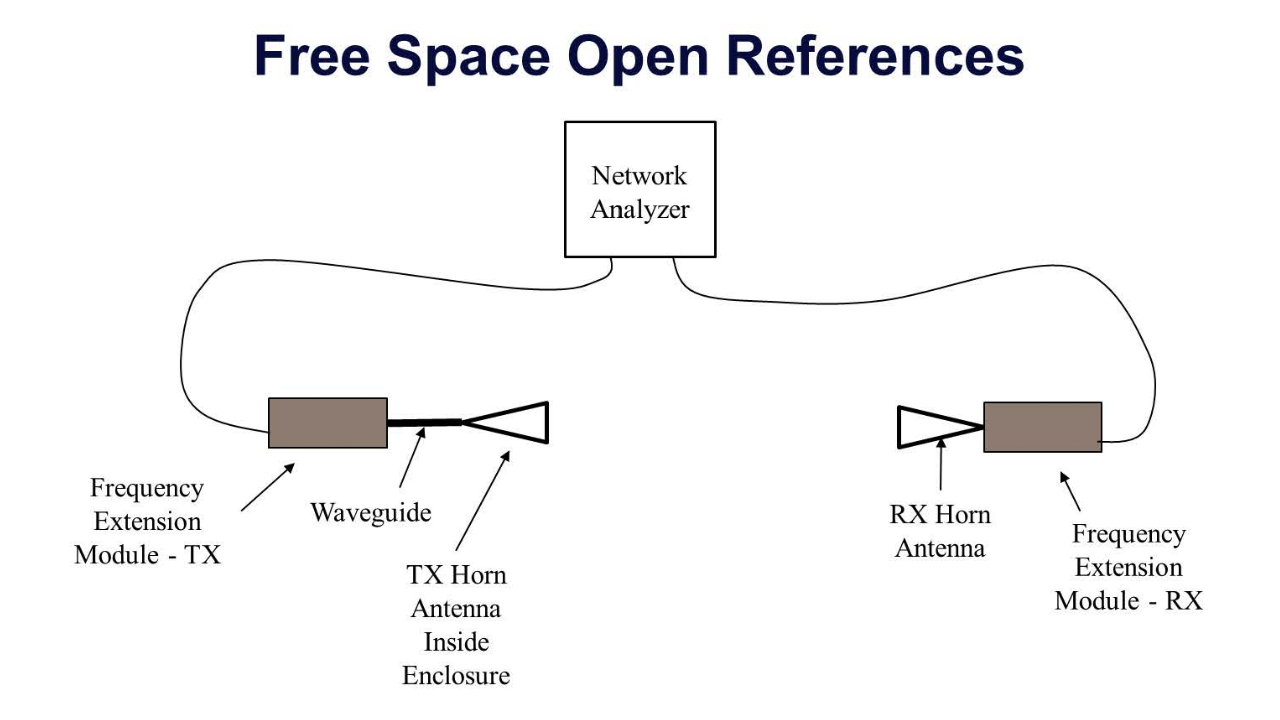
IEEE STD 299 Reference Measurement Technique
For IEEE STD-299 testing in the Main chamber and using the Parker Chomerics Mini Box, testing was performed by using the “Free Space” reference test method shown below. In both cases, the transmit and receive antennas are pointed directly at each other at the same distance apart as in final shielding effectiveness measurements.
Final shielding effectiveness measurements
Final shielding effectiveness testing is done with the test sample in place. Shielding effectiveness is then calculated based on the difference between the value obtained during the open reference measurement and the final measurement and is expressed in decibels (dB).
Test data


Test data discussion
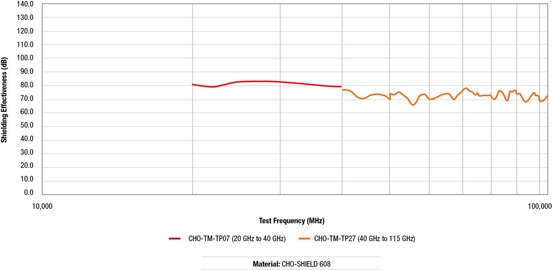
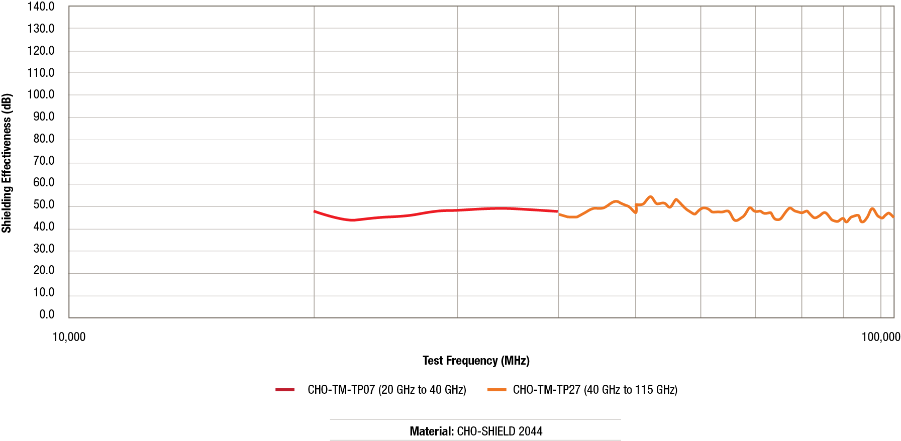
The graphs provide shielding effectiveness test data for the conductive coatings from 18GHz to 115GHz. The graphs combine the test data results from each of the different test methods.
As expected, there are some differences but in general the comparison is exceptional considering the differences in test methods. The test data also impacted by the different antennas, waveguides, waveguide adapters and frequency extension modules used for each band. In addition, antennas used in the different bands create resonates that vary due to the geometry of the enclosure, aperture and antenna distances. These resonates are shown on each graph as larger or smaller peaks and nulls in the data curve. Due to these test conditions, it is recommended to view the test data as a trend line which averages the extremes in data. It’s simply not worth the time and effort to change the test and test method to eliminate this phenomena.
Conclusion
Conductive coatings used in the 5G marketplace are effective solutions in Electromagnetic Compatibility design. Depending on the frequency of interest, Shielding Effectiveness from the conductive coatings can range from 40 to 80dB.
Added Note – Many EMI shielding materials manufacturers present Shielding Effectiveness test data which does not reflect the actual performance of the material in an end application. Any of the test methods presented can be “modified” in a manor not seen it the typical end use application i.e. very small test samples and many mechanical fasteners. These modifications result in unrealistic test data for the material under test.
Parker Chomerics designs and uses shielding effectiveness test fixtures and test methods to BEST reflect the conductive coating product use in an end application. Parker-Chomerics operates under a FULL DISCOLSURE approach in evaluation of our materials. Our experience has been that end users achieve similar shielding effectiveness to that of our published test data.

Author
David Inman
Applications and Test Services Manager
Parker Chomerics
Contributor
Nikolas Antonucci
Engineering Intern
Parker Chomerics
PROVEN PERFORMANCE
Leading the mmWave evolution in 5G and beyond.
We continue to advance technologies to bring new and enhanced capabilities and efficiencies.
EMI Shielding and Thermal Solutions for High Frequency 5G Applications
Major telecom providers are working hard to overcome a range of technical challenges to deliver on 5G’s potential. One of the outcomes of this work will be a higher number of components in more compact spaces, which in turn prompts the need for effective electromagnetic compatibility (EMC) and thermal management solutions.
This Is the Next Generation High Performing Thermal Gap Filler Pad
Looking for high thermal conductivity, yet ultra-soft thermal gap filler pad? Then you’ll want to take a close look at THERM-A-GAP PAD 60, which offers the enticing combination of both excellent thermal conductivity at 6.0 W/m-K, at a softness of 31 Shore 00. This makes THERM-A-GAP PAD 60 more than 40% softer than current-like-performance thermal gap pads from Parker Chomerics.
We’re constantly innovating in our drive to create the most advanced clean energy solutions.

Empowering Your Business on a Global Scale
Parker Chomerics’ manufacturing operations span the globe, allowing us to serve you locally no matter where you are. We understand your unique needs and provide personalized solutions that cater to your specific requirements.
Can't find what you're looking for? Talk to one of our experts.
© Parker Hannifin Chomerics Division 2026
